|
G. Derylo1, J. Estrada1, B. Flaugher1, J. Hamilton2, D.
Kubik1, K. Kuk1 & V. Scarpine1 For the Dark Energy Survey
Collaboration 1Fermi National Accelerator Laboratory, Batavia, Illinois 60510, USA 2Chemistry & Engineering Physics, University of Wisconsin-Plattville, Platteville, WI 53818
(Dated: May 20, 2008)
| SPIE Proceedings Vol. 7018, Advanced Optical and Mechanical
Technologies in Telescopes and Instrumentation Eli Atad-Ettedgui; Dietrich
Lemke, Editors, 701858, DOI: 10.1117/12.789654
|
We describe the results obtained cleaning the surface of DECam CCD detectors with a new electrostatic dissipative formulation of First Contact polymer from Photonic Cleaning Technologies. We demonstrate that cleaning with this new product is possible without ESD damage to the sensors and without degradation of the antireflective coating used to optimize the optical performance of the detector. We show that First Contact is more effective for cleaning a CCD than the commonly used acetone swab.
Introduction: Charge Coupled Devices (CCDs) are extensively used as photon
detectors in optical astronomical instruments. They are the key components of
imagers and spectrometers all around the globe. See Ref [10] for a
comprehensive description of CCDs. State
of the art detectors have a quantum efficiency (QE) approaching 100% in some wavelengths
and noise levels of a few electrons which allow for a statistically significant
detection of very low signal levels. Future projects, such as DES [1] and Pan-STARRS [2], expect to produce photometric measurements of
astronomical objects with less than 1% uncertainty using CCDs. The surface of
the detectors exposed to light must be extremely clean to avoid degrading the performance
of the CCD. Both light collection efficiency and precision are affected by
contamination in the surface. For these reasons, CCDs are typically handled in clean
rooms, and extreme care is taken to avoid contamination of any kind. In the event of
contamination, for example, condensation of particles on the CCD surface in the
event of a vacuum accident, the illuminated back-side surface of the CCD can be
cleaned with acetone using a static dissipative polyester-tipped cleanroom
swab. This has been done by addition of a small amount of acetone to the tip of
the swab and then manually brushing the surface, with frequent swab changes.
Although mostly effective, this technique is not fully satisfactory. It does
not always remove all contaminants. Some spots have been observed to be
well-adhered to the CCD surface and have resisted removal. A special
formulation of the First Contact cleaning product has been investigated as a potential tool for CCD cleaning. This product, originally developed for the cleaning of precision optics, can be dabbed on as a liquid polymer and allowed to harden. The resulting plastics film can then be peeled off and has been developed such that it removes dust, fingerprints, and residue from the surface. The standard formulation of this product, however,
is not static-dissipative and can generate several thousand volts when the film
is peeled from a surface. With the extreme sensitivity of the CCDs to
electrostatic damage, this characteristic of its performance makes it
unsuitable for this work. However, a research effort by the manufacturer has
resulted in a revised formulation of this product that includes the addition of
carbon nanotubes in order to add a small amount of electrical conductivity to
the polymer. Inspection of the film’s surface resistivity indicates that it has
a value of 1010 Ʊ/sq, which puts it slightly into the static-dissipative
category. A sample of the film without the carbon nanotubes was found to have a
resistivity of greater than 1012 Ʊ/sq, classifying it as an insulator. The Detectors: Recent advances [4] in CCD technology allow the fabrication of devices approximately 300 μm thick which are fully
depleted at relatively low voltages. These CCDs have a significantly higher
efficiency in the near-IR and for this reason are the optical detectors chosen
by several groups building new mosaic cameras for astronomy, such as DECam [1,
5] , SNAP [6] and HyperSuprime [7]. A cartoon of the devices used in the
cleaning tests is shown in Fig. 1. It is a back illuminated, p-channel CCD thinned
to 250 μm and biased from the back side to be fully depleted. An antireflective
(AR) layer is applied to the back of the detector to optimize its performance
in a wide range of wavelengths. The CCDs used in most astronomical instruments
until now are thinned to <40 μm to reduce charge diffusion. For the DECam
CCDs, a substrate voltage of up to 80 V is applied to the back surface to
control diffusion and obtain acceptable image quality in 250 μm detectors. Here,
we present the results obtained with a new cleaning technique used on the DECam
detectors [5, 8, 9]. DECam is the instrument currently being built for the Blanco
4m Telescope at CTIO [11] that will be used for the Dark Energy Survey (DES)
and will be available as a facility instrument at CTIO.
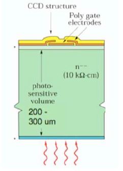
Fig 1. Schematic of a DECam dectector. Back illuminated, 250 μm thick, p-channel CCD. For more details see Ref. [4]
Cleaning with First Contact Polymer: First Contact optics
cleaning polymer has been used to clean the light-collecting surface of several DECam CCDs.
The cleaner is a proprietary liquid polymer that is dabbed directly onto the
CCD surface where it hardens into a solid film. When peeled off, small
particles and organic residues on the surface are removed along with the film. During
the CCD cleaning process, a small quantity of the polymer was first dispensed
into a conductive dish that could be positioned in the work area close to the module.
A long-bristled brush was then dipped in the solution and withdrawn, leaving a
droplet at the end of the brush. This droplet was gently brought into contact
with the surface of the CCD in such a way that the polymer droplet, not the
brush itself, contacts the surface. Lateral brush motion then drags the droplet
around, coating a section of the surface. Initially, the polymer was
carefully applied around the perimeter of the sensor. The care required with
this technique when working near the sensor edges, along with the desire to
avoid having any of the polymer flow over the edge of the silicon, meant that
the applied polymer did not always reach the diced edge of the sensor. The DES
sensors have a perimeter of about a millimeter of inactive silicon around the
edge of the active pixel area, which reduces the criticality of this issue.
Once the polymer was successfully applied around the perimeter, the interior
portion bounded by the dam can be coated using the same technique but with less application
precision. Care was still taken, however, to keep the polymer droplet,
and not the application brush, in contact with the CCD surface. Once coverage
was complete, some type of feature had to be added to the coating to aid removal once it
has solidified. For this purpose, a short length of cotton string was placed on
the coating such that a portion of the string extended off a corner of the
sensor. Additional polymer was applied on top of the string in order to
encapsulate it in place. The polymer was then permitted to solidify overnight.
An example of a CCD at this stage is shown in the middle panel of Fig. 2.Removal
of the resulting solid polymer film was initiated in the corner with the
string, first with a sharp tool inserted into the polymer encapsulating the
string in this region. Once the corner has been started, the string can be
pulled back very slowly to peel the polymer off the CCD surface
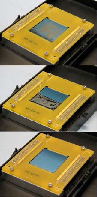
FIG. 2: Cleaning of the DECam 2x2 picture frame CCD. Top) Detector
after losing vacuum while cold, Middle) Detector being cleanned and Bottom)
result for the cleaning process.
Results:
Cleaning
of an inactive region of a CCD wafer
Our
first experience with First Contact consisted
of cleaning an inactive corner of a CCD wafer. For this experiment we used the
standard First Contact polymer, not
suitable for detector cleaning because it is not conductive and could build up
a significant amount of electrostatic charge. The wafer corner piece was first
cleaned using an acetone swab.
Several drops of acetone were applied directly to the silicon (something not commonly
done for CCDs) and allowed to dry before the residue was swabbed off as much
as possible, resulting in several remaining residue features when viewed under
magnification. We then recorded images of 15 locations on the CCD using a microscope
with an X/Y coordinate positioning system. The piece was then cleaned with
First Contact and imaging of the same 15
regions was repeated. An example image is shown in Fig. 3, where the efficiency
of First Contact in removing the acetone
residues is evident.
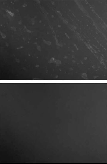
FIG. 3: Microscopic images of a wafer after cleaned with acetone (top) and after the application of First Contact (bottom). The image width is approximately 340 μm.
Electrostatic
safety of the cleaning process A
modified version of First Contact was
doped by the manufacturer with carbon nanotubes to give a small amount of
electrical conductivity, making it static dissipative. The
next step before cleaning a scientific grade CCD with First Contact was to certify the ESD safety of this product
specially developed for electrostatic sensible components. We cleaned 4
engineering grade 0.5 k x 1 k detectors using First Contact with carbon nanotubes. These small devices are
part of the production wafer of DECam detectors and are usually used as test
detectors since they are too small for the DECam instrument. Three of the
sensors showed no problem after cleaning, which gave us confidence in the ESD
safety of the procedure. The fourth detector had a problem with one amplifier
after cleaning, but this problem could have been produced during handling steps
not directly related to the cleaning. Based on these tests, we gained enough
confidence in the static charge dissipation provided by the carbon nanotubes
and decided to start using First Contact for detectors of greater value.
Cleaning
of 2k x 2k detector (pb-22-04)
After
certifying the ESD safety of First Contact with nanotubes, we decided to use the product
to clean a 2k x 2k scientific grade detector. The detector was operational after
the cleaning process and we investigated the incidence of cosmetic defects in
the image before and after cleaning. An example of the type of artifacts coming
from contamination removed by First Contact is shown in Fig. 4. Another concern when
cleaning a CCD imager with any product is the possible damage to the surface
exposed to
light. This surface has an antireflective coating to produce optimal
performance in a desired wavelength range. We investigated the effect of First
Contact on this AR coating by measuring
the QE of the detector before and after cleaning. The results are shown in Fig.
5, demonstrating no degradation of the surface after cleaning with First
Contact.
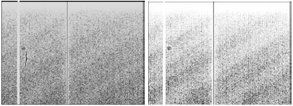
FIG.
4: 300 pixel wide region of a CCD image before (left) and after (right)
cleaning with First Contact. A small fiber is efficiently removed from the
surface during the cleaning process. Each pixel is 15 μm x 15 μm. Both images
shows a hot column and a blocked column. These are produced by cosmetic defects
in the Si
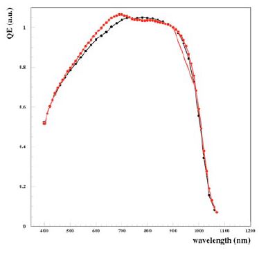
FIG.
5: Relative Quantum Efficiency mesurement before (black) and after (red)
cleaning with First Contact. There is no evidence of any degradation in the AR
coating after the cleaning
Cleaning
of 2k x 2k detector after vacuum accident (pb-22-01)
The
testing chamber where we operated a 2k x 2k DECam CCD lost vacuum while the
detector was at -100 C. The pump accidentally vented, allowing air to come into
our detector chamber while the detector was still cold. This produced
condensation of the humidity in the air, and any contaminants in the air, onto
the cold surface of the detector This type of accident is a common cause of contamination
in astronomical instruments. After
this accident, the surface of the detector looked extremely dirty as shown on
the top panel in Fig. 2. The detector was cleaned using two techniques. The
upper half was cleaned with an acetone swab and the lower half was cleaned with
First Contact . The bottom panel in Fig. 2 shows a photograph of the detector
after cleaning. The cleaned surface was inspected using an optical microscope and
the results are shown in Fig. 6 and Fig. 7. The width of each microscope image
is about 340 microns. Figure 6 shows the results of cleaning using both methods
in the bulk (central region) of the imager. For the acetone
swab there is some residue of the original contamination, seen as white spots
in the image. For the region cleaned with First Contact there is no remnant of the original
contamination. Figure 7 shows the results for the edge of the CCD. When the
edge is cleaned with the acetone, the results are very similar to that observed
in the bulk of the detector. However, it was more difficult to apply the First Contact
polymer all the way to the edge of the
sensor. Some small amount of
contamination at the very edges therefore
still exists, as can be seen in Fig. 7. The QE was measured for the region
cleaned by First Contact and the region
cleaned with acetone. The results indicate that, when compared to the region
cleaned with acetone, there was no degradation of the QE (therefore no damage
to the AR coating) by cleaning with First Contact . In addition, the device
still meets the DECam technical requirements for QE.
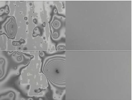
FIG.
6: Results of cleaning with acetone (top) and with First Contact (bottom) on
the bulk (central region) of the CCD imager. The left images are before
cleaning; the images on the right are after cleaning. After the acetone
cleaning one can see some contamination as white features in the image, that
are completely removed with First Contact
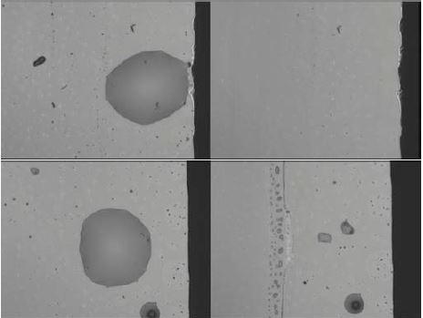
FIG.
7: Results of cleaning with acetone (top) and with First Contact (bottom) on
the edge of the CCD imager. The left images are before cleaning; the images on
the right are after cleaning. The application of First Contact to the edge of the
detector is difficult and some residue remains compared with the acetone swab.
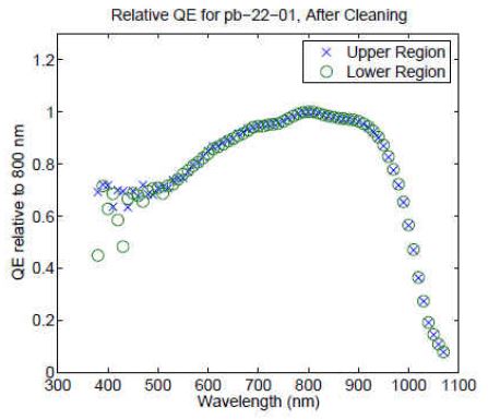
FIG.
8: QE of the upper half of the CCD which was cleaned with acetone and QE of the
lower half of the CCD which was cleaned with First Contact the detector is
difficult and some residue remains compared with the acetone swab
Cosmetic
defect statistics
CCDs
used for astronomical devices are typically graded according to the fractional
area compromised by cosmetic defects. This grading is used to select the best detectors
to be used in an instrument. Cosmetic defects in CCDs are isolated pixels,
groups of pixels, or columns that exhibit poor image quality. Defects include
pixels that generate charge at a higher rate than the average in an array
(white spots) and pixels with lower photo-response than average (black spots). The
black spots are measured in high signal to noise images of detectors uniformly
illuminated (flat field), and white spots are detected using long dark
exposures at the operating temperature. White spots may be caused by impurities
in the silicon, lattice defects, or shorts through the gate oxide. Mechanical
damage is one cause of oxide shorts. On back illuminated devices (like those
used in the First Contact tests), black
spots can be caused by scratches or imperfections in the anti-reflective
coating. Therefore, the number of cosmetic defects can be used as a measure of whether
the First Contact cleaning procedure
caused any damage to the CCD. Black spots may also be caused by opaque dirt or
dust on the surface of the CCD. Again, a count of cosmetic defects can be used
to indicate the effectiveness of cleaning with First Contact . An example of a
cosmetic feature removed with First Contact is shown in Fig. 9.
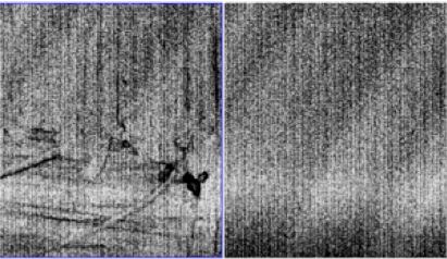
FIG.
9: CCD image resulting from a flat field illumination of a 2k x 2k CCD before
cleaning with First Contact (left) and after cleaning with First Contact TM
(right).
The dark areas are on the
order of 3% below background. Cleaning this 2k x 2k device (pb-22-04 mentioned
above) with First Contact reduced the
percent of pixels whose response was more than 3% below background by one half:
from 1.6%
to 0.8%. Note that our standard cosmetic analysis defines dark pixels as those
with a response more than 20% below background. The fraction of pixels affected
by cosmetic defects for the CCD that was cleaned after the vacuum accident (pb-22-01
above) was 0.09%, well below the DECam requirement of less than 2.5% per CCD.
The defects counted were white spots (pixels with dark current greater than 6300
e-/pixel/hour) and black spots (pixels with a response more than 20% below
background). While the total number of white spots was similar for both the top
half (cleaned with acetone) and the bottom half (cleaned with First Contact ),
all of the black spots were located on the half cleaned with acetone. This
implies that First Contact may be more
effective than the acetone swab for removing opaque dirt or dust on the CCD
surface and that cleaning with First Contact did not damage the CCD. Cleaning with First
Contact converted the dramatically
contaminated detector shown in Fig. 2 into a scientific grade CCD.
Conclusion:
We have tested the recently-developed ESD-safe version of the First Contact cleaning polymer on several DECam CCD devices
and found improvements in image cosmetics with no degradation of collection
efficiency. The charge dissipation of the product provided by the addition of
carbon nanotubes is effective in reducing the risk of ESD damage during the
cleaning of these very sensitive devices. During these tests we also verified
that, as expected, cleaning did not degrade other performance parameters of the
CCDs, such as linearity or charge transfer efficiency. In our tests, the
product removed contamination from the CCD surface more effectively than
swabbing with acetone,
which does not remove all contaminants and which can leave behind some residue.
Tests on a sensor which had been contaminated by loss of vacuum while cryogenically
cooled found that the contaminants were effectively removed except near the
very edge of the sensor, where complete coverage with the polymer was found to be
difficult due to the delicate nature of the CCD module and the care necessary
in this area.
[1]
Dark Energy Survey Collaboration, astro-ph/0510346.
[2]
pan-starrs.ifa.hawaii.edu/public/
[3]
www.photoniccleaning.com/
[4]
S.E. Holland, D.E. Groom, N.P. Palaio, R. J. Stover, and M. Wei, IEEE Trans.
Electron Dev., 50 225 (2003), LBNL-49992.
[5]
Flaugher, B., Ground-based and Airborne Instrumentation for Astronomy. Edited
by McLean, Ian S.; Iye, Masanori. Proceedings of the SPIE, Volume 6269, (2006)
[6]
“Supernova / Acceleration Probe: A Satellite Experiment to Study the Nature of
the Dark Energy”, SNAP Collaboration, G. Aldering et al., submitted to Publ. Astr.
Soc. Pac., astro-ph/0405232; SNAP Collaboration, astro-ph/0507459.
[7]
M. Satoshi et al., Ground-based and Airborne Instrumentation for Astronomy.
Edited by McLean, Ian S.; Iye, Masanori. Proceedings of the SPIE, Volume
6269, (2006)
[8]
J. Estrada & R. Schmidt , Scientific Detectors for Astronomy 2005, Edited
by J.E. Beletic, J.W. Beletic and P. Amico, Springer, (2006).
[9]
J. Estrada et al. , Ground-based and Airborne Instrumentation for Astronomy.
Edited by McLean, Ian S.; Iye, Masanori. Proceedings of the SPIE, Volume 6269,
(2006).
[10]
J.R. Janesick, Scientific Charge Cupled Devices, SPIE press (2001).
[11]
T. M. C. Abbott et al. ,Ground-based and Airborne Instrumentation for
Astronomy. Edited by McLean, Ian S.; Iye, Masanori. Proceedings of the SPIE,
Volume 6269, (2006)
[12]
H. Cease, H. T. Diehl, J. Estrada, B. Flaugher and V. Scarpine, Experimental
Astronomy , Online First (2007)
|
|
|